The purpose of the introductory assignment is to familiarize students with HDL design and CAD tools, including a review of the Logical Systems lecture and Experiment 2 Hardware. There will also be a special emphasis on proper report writing.
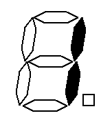
A 7SEG LED (shown below) is a commonly used device for displaying numerical values including the hexadecimal numbers A-F. The device consists of eight LEDs.
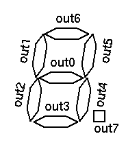
Usually, 7SEG LEDs are used in combination with a decoder, which accepts a single hexadecimal digit (4 bits) input and displays the corresponding hexadecimal digit (0-F). However, 7SEG LEDs on the PowerMedusa board used in Experiment 3 Hardware are not equipped with a decoder so that they can be used for applications other than hexadecimal representation. To that end, the FPGA outputs are connected to each of the 8 LEDs within each single 7SEG LED.
This assignment is to design a combinational circuit that accepts this single hexadecimal digit (4 bits) input and displays 0 to F by lighting up the 8 LEDs on MU500-RK appropriately. (LEDs on MU500-7SEG are acceptable for AY2022 only. If you use MU500-7SEG, please specify in the report.) Also, using this circuit as a component, you will design a sequential circuit to display a count.
Design a circuit that inputs 4-bit data from a PowerMedusa input device and displays a one-digit hexadecimal number on a 7SEG LED, then verify that it works correctly on the board.
First, to represent a single hexadecimal digit from 0 to F using a 7SEG LED, consider how to display it. For example, the representation of "1" is shown in the figure below.
In the report, include a description of how you decided to express 0 to F.
A single hexadecimal digit is represented by 4-bit.
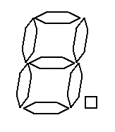
Design a combinational circuit that takes 4-bit input and outputs an 8-bit signal to drive a 7SEG LED as shown in the figure below.
Your report needs to show your reasoning behind how the logic circuit was designed, with an explanation of the HDL code if necessary.
The input/output pins must be specified so that 4 bits are input from the input device on the board and a one-digit hexadecimal number is displayed on the 7SEG LED. You may choose any input device you wish.
Your report must include an explanation of the reasoning behind your design (components used, pin designations, etc.).
First, you will verify that the circuit you designed works properly through a simulation.
Next, you need to download the circuit to the FPGA and verify that it works correctly.
In the report, describe how you verified the operation (you may include testbench code) and that it worked (or did not work) correctly.
Evaluate the performance of the circuit, including circuit size and available operational speed.
Discuss the results of this evaluation to determine if they are sufficient and to consider points for improvement.
Design a circuit that displays four decimal digits and counts up by one at regular intervals, and verify its operation on the board. Examine the performance of the designed circuit, including its size (number of logic elements used) and the speed at which it can operate (maximum clock frequency).
The circuit in Assignment 1 can be called and used as a module. Refer to the FAQ page for details on how to understand the circuit performance. In the report, as was the case in Assignment 1, explanation will be provided on specifications decision, logic design, CAD design, operation result verification and performance evaluation including discussions on each.
Add an input from a switch on the board to the circuit in Assignment 2 so that counting up can be stopped/restarted each time the switch is pressed. (Note that you will need to deal with switch chattering)
Report Check Sheet for TA (txt format, UTF-8, In Japanese)
In other words, it is expected that the items in this checklist are completed in the report you submit.